

Photovoltaic solar
It is estimated that at latitudes in France, around 45 °, the potentially usable energy of the sun is 1500kwh / m² per year.
See the French sunshine map and l'DNI solar irradiation from France.
With current yields of about 10 to 15% we get from 150 to 225kwh / m².an.
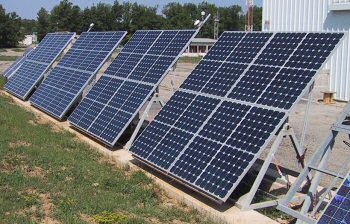
So-called “non-integrated” solar panels.
Operating principle of photovoltaics
A photovoltaic cell is made of semiconductor materials. These are able to transform the energy provided by the sun into an electric charge and therefore into electricity because the sunlight excites the electrons of these materials. The absorption curve of these materials starts from low wavelengths up to a limiting wavelength which is 1,1 micrometers for silicon.
Silicon is the main component of a photovoltaic cell.
Physics of a photoelectric cell (taken from the CEA website)

Functional diagram of a photoelectric cell.
Silicon was chosen to make photovoltaic solar cells for its electronic properties, characterized by the presence of four electrons on its peripheral layer (column IV of Mendeleiev's table). In solid silicon, each atom is bonded to four neighbors, and all the electrons in the peripheral layer participate in bonds. If a silicon atom is replaced by an atom from column V (phosphorus for example), one of the electrons does not participate in the bonds; it can therefore move around the network. There is conduction by an electron, and the semiconductor is said to be n-type doped. If, on the contrary, a silicon atom is replaced by an atom from column III (boron for example), an electron is missing to make all the bonds, and an electron can come to fill this gap. We then say that there is conduction through a hole, and the semiconductor is said to be p-type doped. Atoms such as boron or phosphorus are dopants of silicon.
When an n-type semiconductor is brought into contact with a p-type semiconductor, excess electrons in the n material diffuse into the p material. The initially n-doped zone becomes positively charged, and the initially p-doped zone becomes negatively charged. An electric field is therefore created between the n and p zones, which tends to push the electrons back into the n zone and an equilibrium is established. A junction was created, and by adding metal contacts on the n and p areas, a diode is obtained.
When this diode is lit, the photons are absorbed by the material and each photon gives birth to an electron and a hole (we speak of electron-hole pair). The junction of the diode separates the electrons and the holes, giving rise to a potential difference between the contacts n and p, and a current flows if a resistor is placed between the contacts of the diode (figure).


Technologies available on the market.
Current modules are distinguished by the type of silicon they use:
- monocrystalline silicon: photovoltaic sensors are based on silicon crystals encapsulated in a plastic envelope.
- polycrystalline silicon: Photovoltaic sensors are based on silicon polycrystals, which are less expensive to manufacture than monocrystalline silicon, but which also have a slightly lower yield. These polycrystals are obtained by melting scrap of silicon of electronic quality.
- amorphous silicon: the “spread” panels are made with amorphous silicon with high energizing power and presented in flexible strips allowing perfect architectural integration.
Cell builders.
The five largest firms manufacturing photovoltaic cells share 60% of the world market. These are the Japanese companies Sharp and Kyocera, the American companies BP Solar and Astropower, and the German RWE Schott Solar. Japan produces almost half of the world's photovoltaic cells.
Solar Electric Power Applications
Currently the main areas of use are isolated dwellings but also for scientific devices such as seismographs.
The first domain to have used this energy is the space domain. Indeed, almost all the electrical energy of the satellites is provided by photovoltaics (some satellites have small stirling motors).
Benefits
- Non-polluting electrical energy in use and is part of the principle of sustainable development,
- Renewable energy source because it is inexhaustible on a human scale,
- Can be used either in developing countries without an important electricity network or in isolated sites such as in the mountains where it is not possible to connect to the national electricity network.

Example of an isolated site supply, a seismograph powered by a photovoltaic panel from the Soufrière volcano in Guadeloupe.
Drawbacks
- Photovoltaic cost is high because it comes from high technology,
- cost depends on the peak power, the current cost of the peak watt is around 3,5 € or around 550 € / m² of solar cells,
- the current yield of photovoltaic cells remains fairly low (around 10% for the general public) and therefore only delivers low power,
- market very limited but in development
- electricity production is only done during the day while the highest demand is at night,
- storing electricity is very difficult with current technologies (very high ecological cost of batteries),
- lifespan: 20 to 25 years, after the silicon "crystallizes" and renders the cell unusable,
- pollution during manufacturing: some studies claim that the energy used to manufacture cells is never profitable during the 20 years of production,
- likewise at the end of life: the recycling of cells poses environmental problems.
More:
- Energy balance of solar photovoltaic
- Map of French solar field
- Photovoltaic solar systems integrated into the building (CEA document)